🖼️ Image unavailable www.kitguru.net Image #2 Toshiba's 48layer BiCS 3D NAND enables fast and reliable SSDs KitGuru www.kitguru.net Source ↗
🖼️ Image unavailable www.eeworldonline.com Image #3 3D NAND Flash memory Making HDDs obsolete in a datacentric world www.eeworldonline.com Source ↗
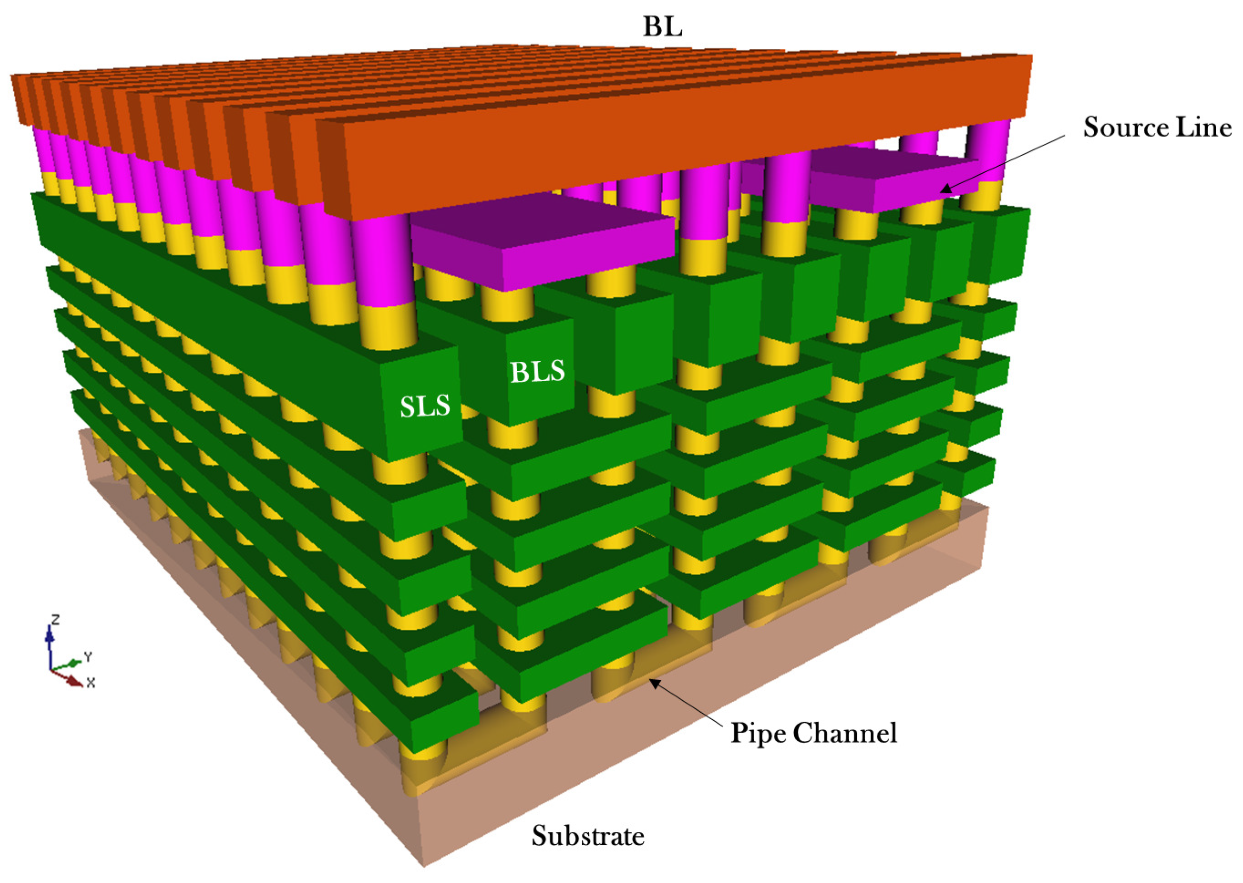
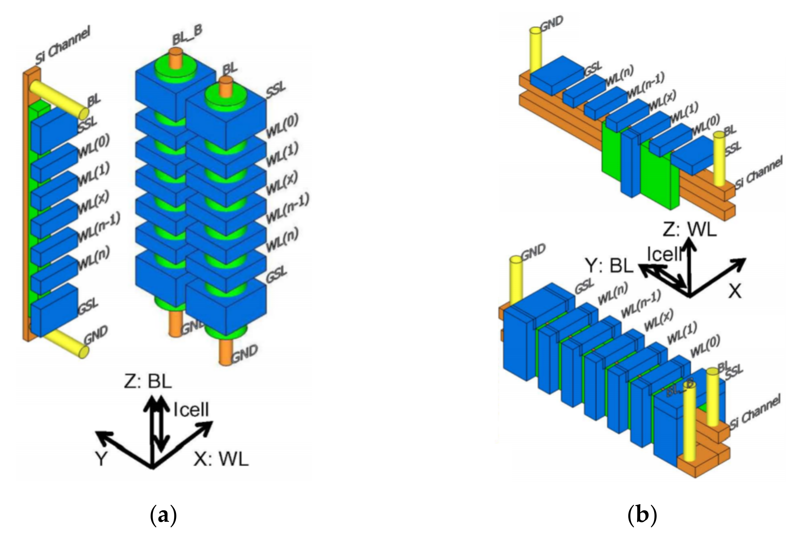
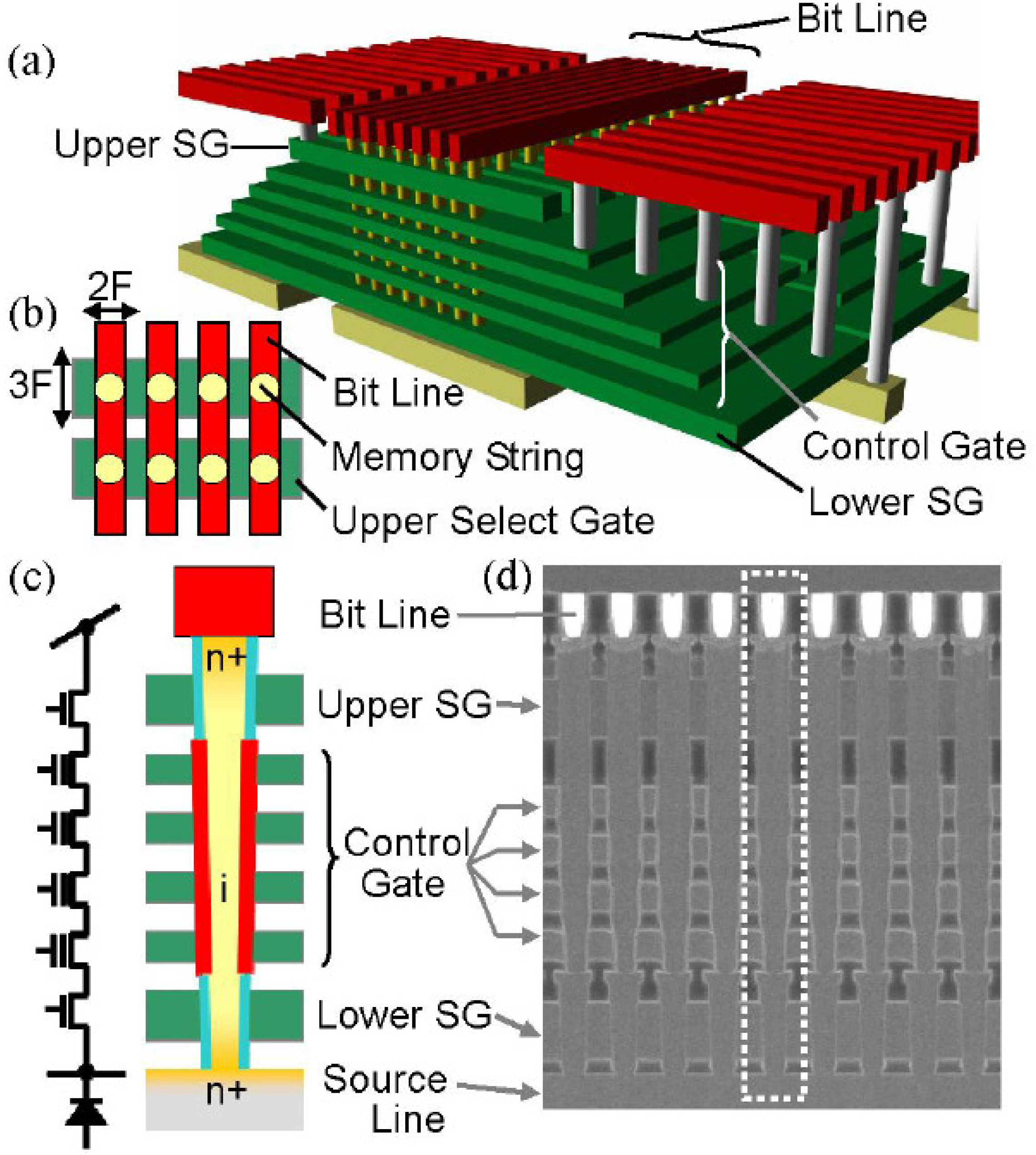
🖼️ Image unavailable www.mdpi.com Image #4 Architectural and Integration Options for 3D NAND Flash Memories www.mdpi.com Source ↗
🖼️ Image unavailable www.techpowerup.com Image #5 Micron and Intel Unveil New 3D NAND Flash Memory TechPowerUp www.techpowerup.com Source ↗
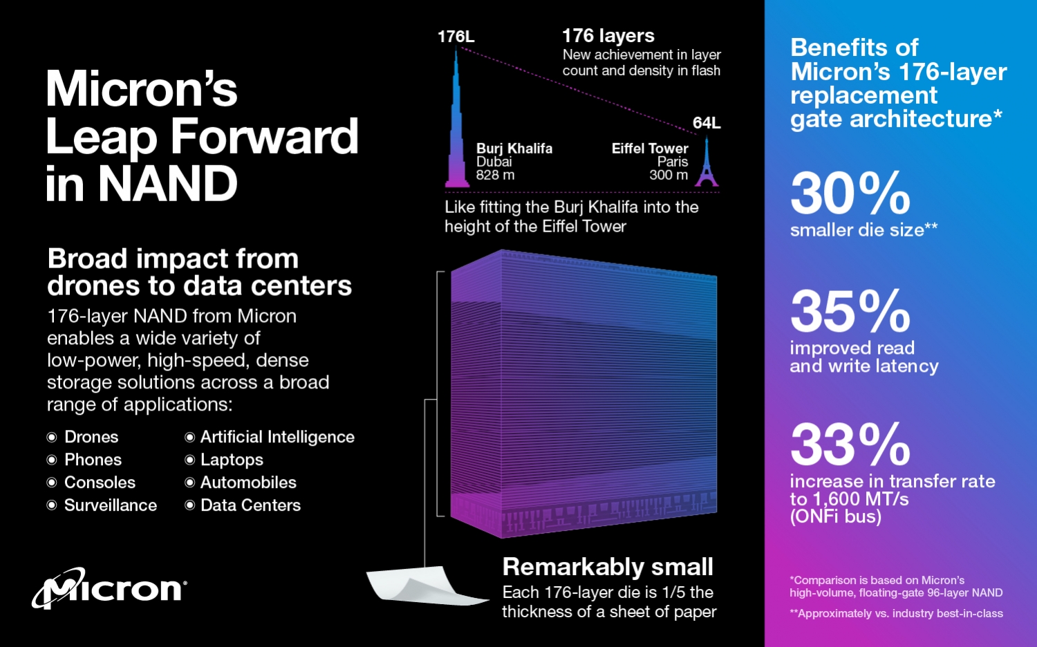
🖼️ Image unavailable www.tweaktown.com Image #6 Micron reveals world's first 176layer 3D NAND flash memory www.tweaktown.com Source ↗
🖼️ Image unavailable www.thermofisher.com Image #7 3D NAND Flash 3D NAND Flash Technology Illuminating Semiconductors www.thermofisher.com Source ↗
🖼️ Image unavailable semiengineering.com Image #8 Semiconductor Engineering 3D NAND Flash Wars Begin semiengineering.com Source ↗
🖼️ Image unavailable www.researchgate.net Image #9 PBiCS 3D NAND Flash array. Download Scientific Diagram www.researchgate.net Source ↗
🖼️ Image unavailable www.allaboutcircuits.com Image #10 The Rise of Toshiba’s New 3D NAND Flash Memory News www.allaboutcircuits.com Source ↗
🖼️ Image unavailable semiengineering.com Image #11 3D NAND Flash Wars Begin semiengineering.com Source ↗
🖼️ Image unavailable www.mdpi.com Image #12 Architecture and Process Integration Overview of 3D NAND Flash Technologies www.mdpi.com Source ↗
🖼️ Image unavailable www.mdpi.com Image #13 Architecture and Process Integration Overview of 3D NAND Flash Technologies www.mdpi.com Source ↗
🖼️ Image unavailable www.cell.com Image #14 Material engineering to enhance reliability in 3D NAND flash memory Device www.cell.com Source ↗
🖼️ Image unavailable www.assured-systems.com Image #15 Industrial SSD 3D NAND Technology SLC, MLC, TLC www.assured-systems.com Source ↗
🖼️ Image unavailable www.mdpi.com Image #16 A Review of Cell Operation Algorithm for 3D NAND Flash Memory www.mdpi.com Source ↗
🖼️ Image unavailable www.imec-int.com Image #17 Imec improves memory window of a 3D trench cell for nextgen NAND Flash www.imec-int.com Source ↗
🖼️ Image unavailable www.researchgate.net Image #18 (a) 3D NAND flash memory circuit consisting of vertical strings of NAND www.researchgate.net Source ↗
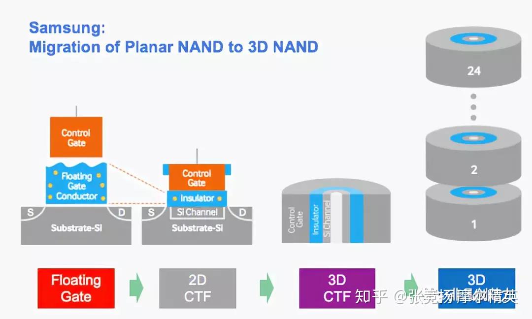
🖼️ Image unavailable zhuanlan.zhihu.com Image #19 你真的懂3D NAND闪存? 半导体行业观察 知乎 zhuanlan.zhihu.com Source ↗
🖼️ Image unavailable www.youtube.com Image #20 28B 3D NAND Memory 3D Structure YouTube www.youtube.com Source ↗
🖼️ Image unavailable techgage.com Image #21 Micron Announces 2nd Gen 64Layer 3D NAND Flash Up To 256GB Chips techgage.com Source ↗
🖼️ Image unavailable www.slideserve.com Image #22 PPT Enhancing Memory Systems with 3D NAND Flash Technology PowerPoint www.slideserve.com Source ↗
🖼️ Image unavailable www.cell.com Image #23 Material engineering to enhance reliability in 3D NAND flash memory Device www.cell.com Source ↗
🖼️ Image unavailable www.storagenewsletter.com Image #24 More on Future of Toshiba 3D NAND Flash Memory StorageNewsletter www.storagenewsletter.com Source ↗
🖼️ Image unavailable electronics360.globalspec.com Image #25 The rise of 3D NAND flash memory Electronics360 electronics360.globalspec.com Source ↗
🖼️ Image unavailable www.getflashmemory.info Image #26 What Is 3D NAND Flash Memory? www.getflashmemory.info Source ↗
🖼️ Image unavailable www.mdpi.com Image #27 Architecture and Process Integration Overview of 3D NAND Flash Technologies www.mdpi.com Source ↗
🖼️ Image unavailable www.cell.com Image #28 Material engineering to enhance reliability in 3D NAND flash memory Device www.cell.com Source ↗
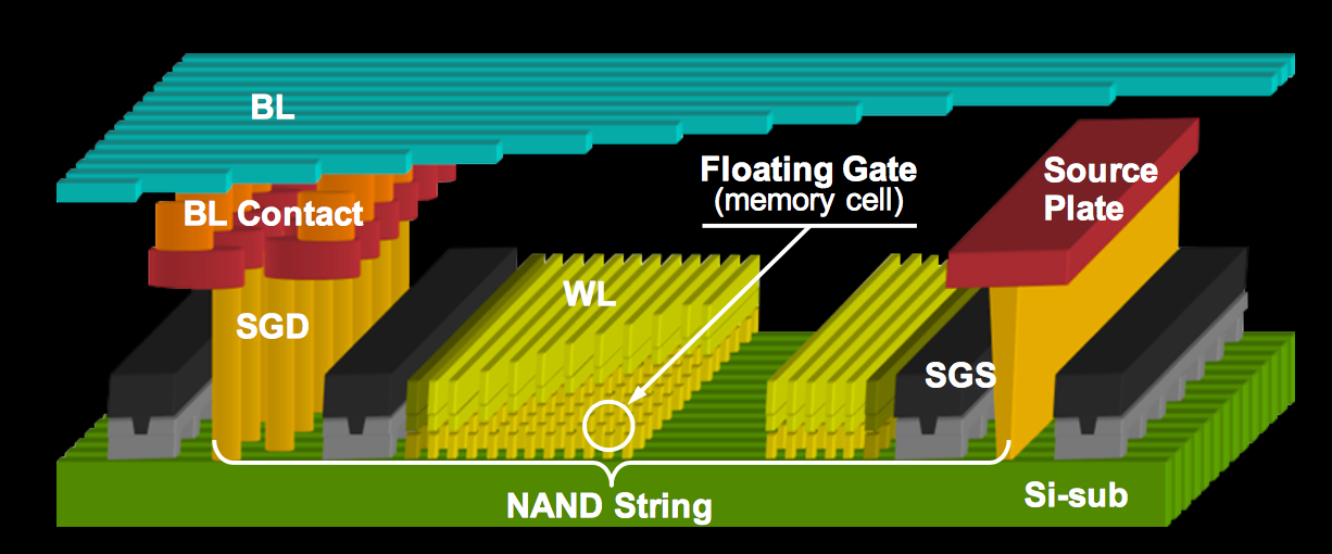
🖼️ Image unavailable www.semanticscholar.org Image #29 3D NAND Memory and Its Application in SolidState Drives Architecture www.semanticscholar.org Source ↗
🖼️ Image unavailable wccftech.com Image #30 218Layer 3D NAND Flash From Kioxia & Western Digital Delivers Huge wccftech.com Source ↗
🖼️ Image unavailable www.mdpi.com Image #31 Architectural and Integration Options for 3D NAND Flash Memories www.mdpi.com Source ↗
🖼️ Image unavailable www.tomshardware.com Image #32 Kioxia and WD Unveil World's Fastest 3D NAND Flash Memory Tom's Hardware www.tomshardware.com Source ↗
🖼️ Image unavailable www.mdpi.com Image #33 Architectural and Integration Options for 3D NAND Flash Memories www.mdpi.com Source ↗
🖼️ Image unavailable www.youtube.com Image #34 [Electronics] 3D structural analysis of a 128layer 3D NAND flash www.youtube.com Source ↗
🖼️ Image unavailable horizontechnology.com Image #35 A Guide To 3D NAND The Persistence of Memory Horizon horizontechnology.com Source ↗


![[Electronics] 3D structural analysis of a 128layer 3D NAND flash — free download](https://i.ytimg.com/vi/458v_J5gQh8/maxresdefault.jpg)